Daniel Morgan
I write code that works (usually).
nand2tetris Part 1: Boolean algebra and logic gates
I've started reading Elements of Computing Systems: Building a Modern Computer from First Principles.
Accompanying website: nand2tetris.org
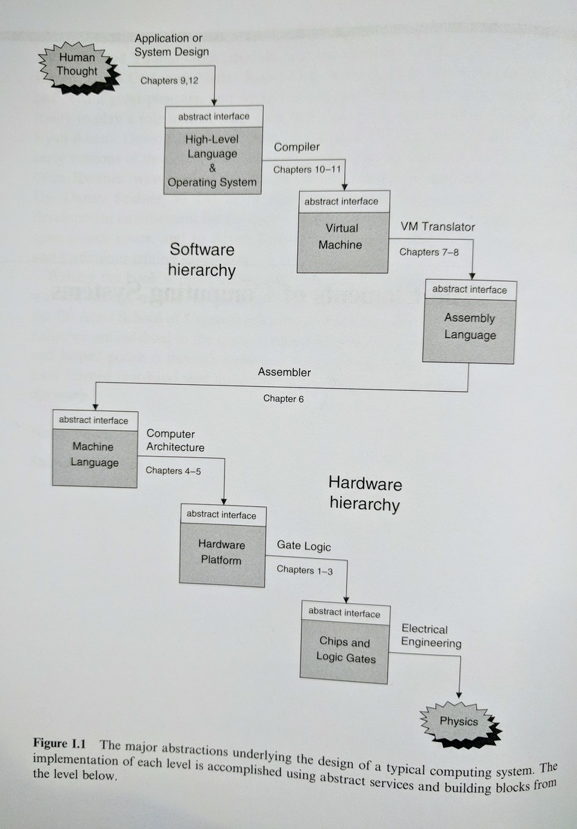
The book presents an interesting idea: From a single type of logic gate, NAND, we can construct more complex gates. From those gates we can build combinational logic to add numbers together or perform bitwise operations on them. Then sequential logic when we introduce a clock signal, which gives us the ability to store information in registers and RAM. Then machine code for programming our computer. And on and upwards from there until eventually you have a computer that you can code Tetris on in a high-level language.
Interestingly, while we can produce more complex logic circuits from NAND gates, we can even produce less complex gates.
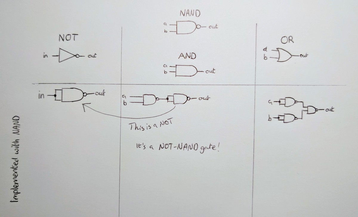
NAND isn't the only fundamental building block you could use: Check out NOR logic.
It's from these 3 simple logical operations: AND, OR, and NOT; that we can start building complex behaviours. The book gives descriptions of more complex chips, along with a truth table describing how it should operate. The course only asks for you to describe a chip in a Hardware Description Language (HDL). It might have been easier if I started there, but I like to have diagrams to really understand what's happening. Below I'll describe the process I came up with to turn truth tables into both diagrams and eventually HDL that runs on the hardware simulator.
Boolean Algebra
The first thing to do is to transcribe the truth table to it's "canonical representation". That means we'll find all the conditions where the result is 1 and OR them together.
In the below truth table row 2 or 3 will result in Q=1.
# XOR truth table

A | B |  Q
-----------
0 | 0 |  0
0 | 1 |  1
1 | 0 |  1
1 | 1 | 0- Row 2: A'.B
- Row 3: A.B'
So we know it has to be row 2 or row 3, and we know how to perform a logical OR:
(A'.B)+(A.B')
Here we've described a simple XOR gate in boolean algebra. Breaking it down:
- A' = Not(A)
- A.B = And(A, B)
- A+B = Or(A, B)
So if we wanted to describe it in a lambda calculus style we could write it:
Or(And(Not(A), B), And(A, Not(B)))
We can draw that out as a circuit diagram pretty easily. Start working outside-in, with the OR gate at the end, the AND gates in the middle, and the NOT gates at the start:
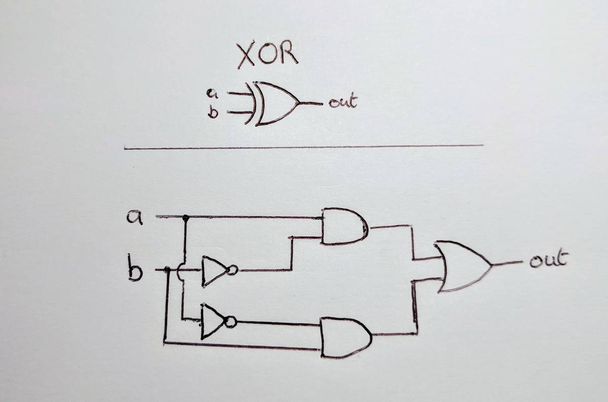
See how we only had to use those 3 basic logic gates? From those we can keep building upwards.
More complex truth tables
For the simpler circuits the Boolean expression comes out quite small, but pretty soon I found myself struggling to take a truth table and figure out the simplest way to write it as an expression. Here's an example:
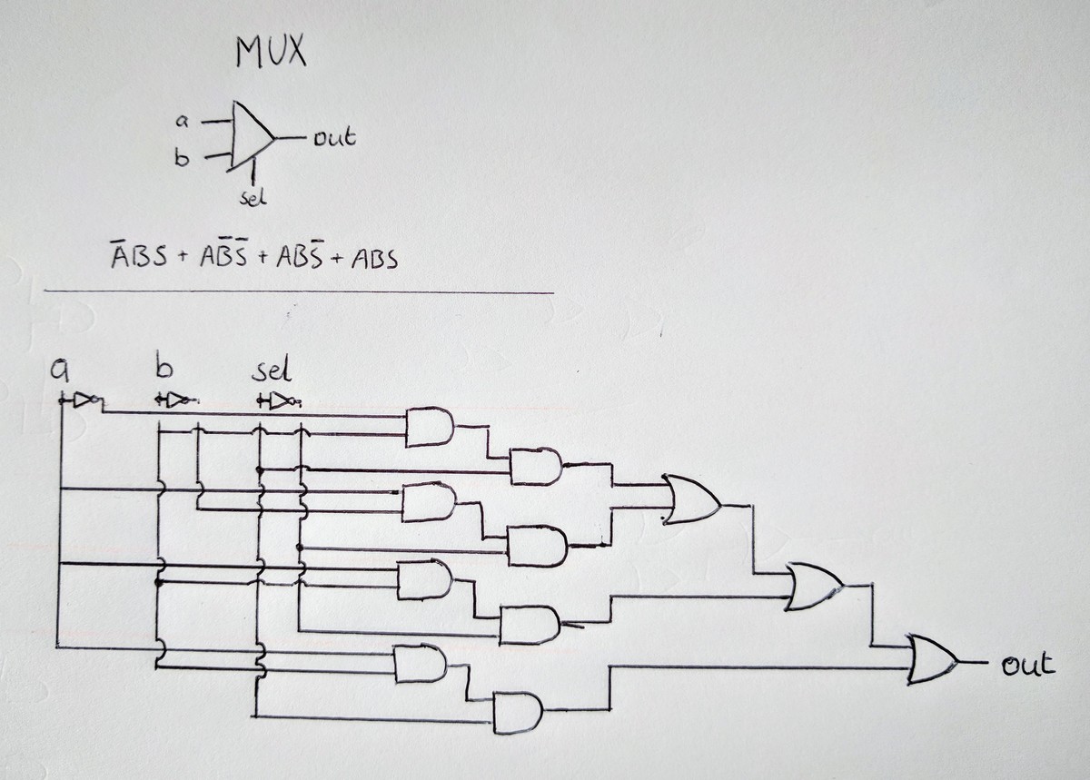
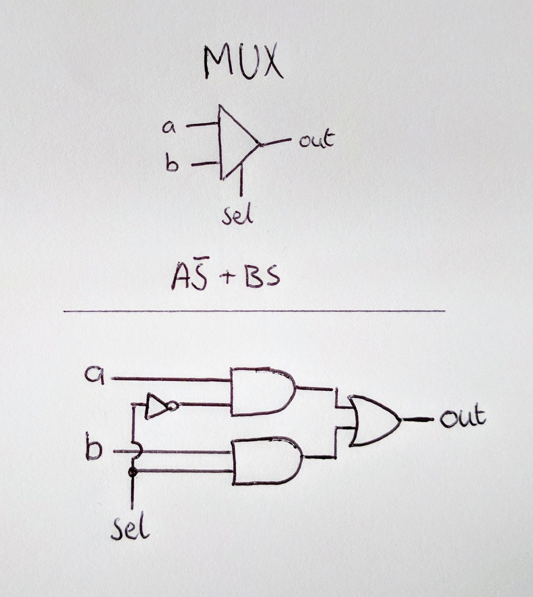
A Multiplexor (Mux) chip takes two inputs, A and B, and outputs one of them. If the select bit S=0, A is output. If S=1, B is output. It might be better named a Switcher.
# MUX truth table

A | B | S |  Q
--------------
0 | 0 | 0 |  0
0 | 0 | 1 |  0
0 | 1 | 0 |  0
0 | 1 | 1 |  1
1 | 0 | 0 |  1
1 | 0 | 1 |  0
1 | 1 | 0 |  1
1 | 1 | 1 |  1
If we pick out the four rows where Q=1, we end up with this expression:
Q=(A'.B.S)+(A.B'.S')+(A.B.S')+(A.B.S)
If we count the number of symbols in that expression (', +, .) we can see we should end up with 15 gates. We can negate S just once and take one of those away for 14 gates. Indeed we see that is the case when we translate it to a circuit diagram:
If our eventual computer platform has thousands of these gates and they're used a lot by our software, then this will significantly slow everything down. Savings made at the electronics level will speed up every layer above it.
This is where I felt the book let me down a bit. It doesn't dive into the boolean algebra too deeply. I did some research of my own and learned a couple of new concepts that gave me the tools I needed to start with a complex truth table and end up with the simplest possible circuit.
Reflected binary
We normally count in binary the same way we count in any number base. After filling up one column we reset it and carry 1 over to the left.
# Binary counting

base two | base ten
----------------
 000     |  0
 001     |  1
 010     |  2
 011     |  3
 100     |  4
 101     |  5
 110     |  6
 111     |  7
An interesting side effect of this is particularly relevant to circuit design. When we reach 3(ten) the binary representation is 011. When we go up one more to 4(ten) then all 3 bits need to flip to 100.
In an electromechanical system this can be an expensive operation. Frank Gray, a researcher at Bell Labs, came up with a system of counting in binary "such that two successive values differ in only one bit". It's called reflected binary (RB), or Gray Code, and looks like this:
# Reflected binary counting

gray code | base ten
--------------------
 000      |  0
 001      |  1
 011      |  2
 010      |  3
 110      |  4
 111      |  5
 101      |  6
 100      |  7
I only learned about RB on a tangent because it's used in the next concept:
Karnaugh map
The K-map "is a method of simplifying Boolean algebra expressions" (wikipedia). Sounds like just the thing. Simpler expression, simpler circuit.
I could try to badly explain this but it's a very visual thing (it takes advantage of our pattern matching ability) so I'll just link you to the series of videos I watched:
Lets use a K-map to simplify our Mux expression:
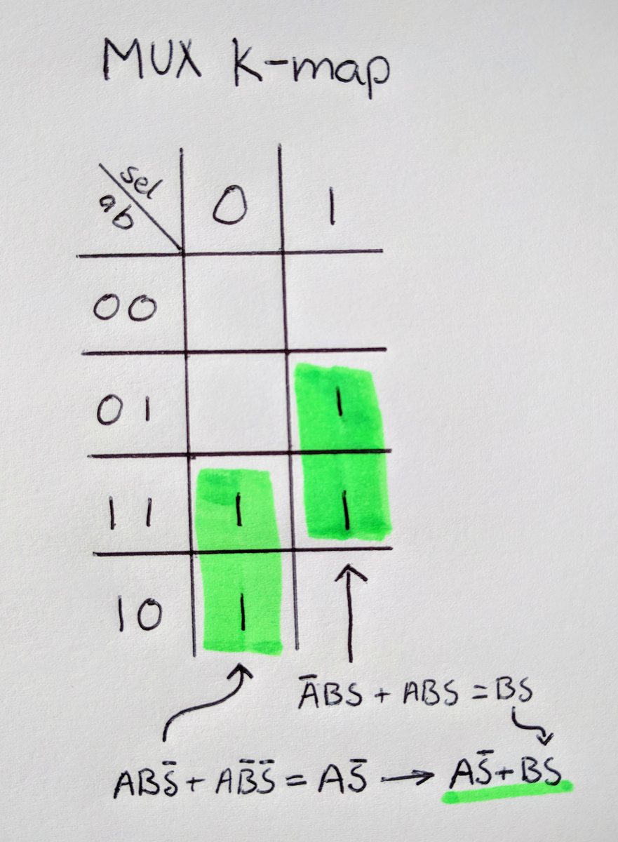
Q=(A.S')+(B.S)
And we end up with a much simpler circuit diagram:
HDL
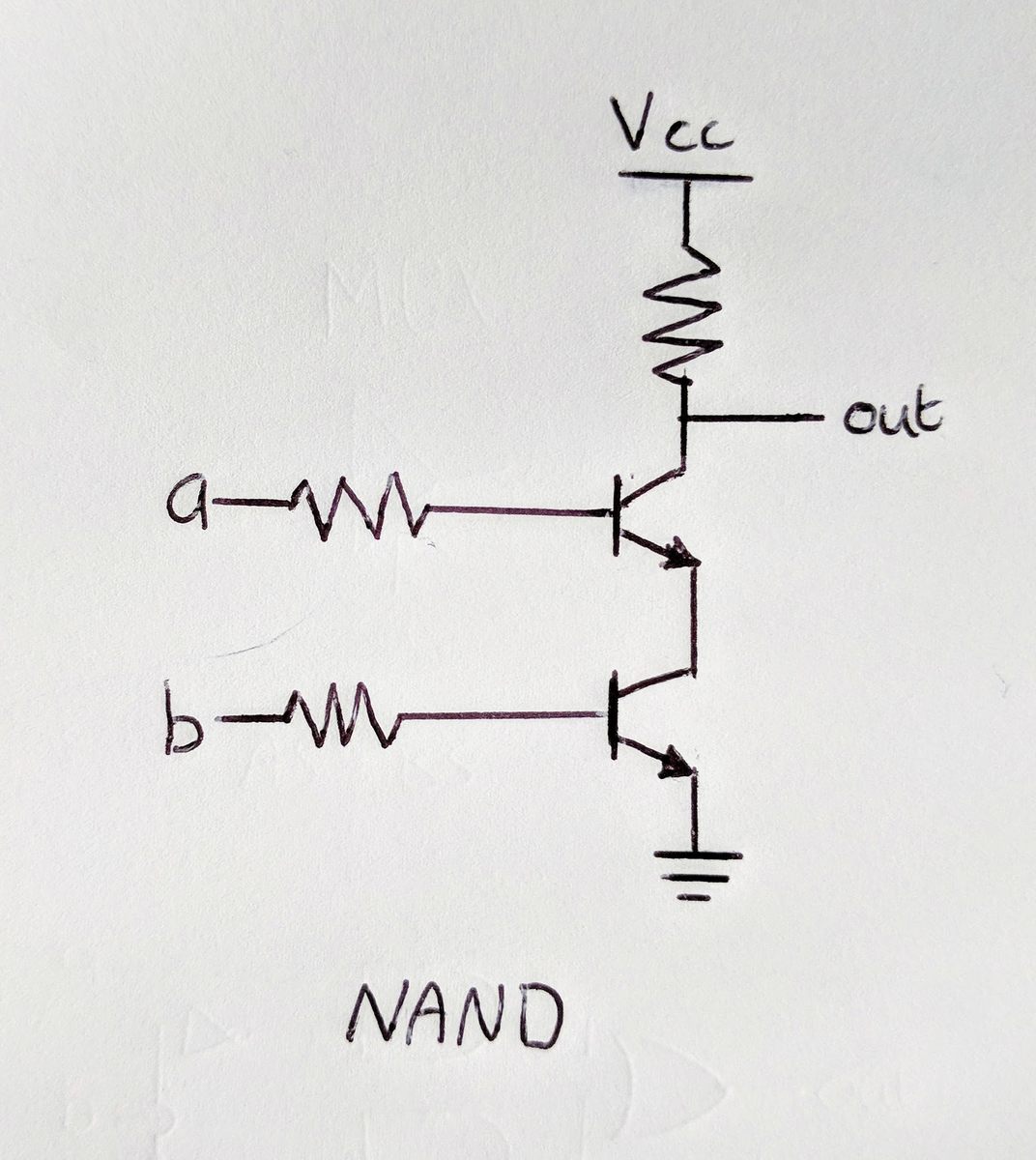
For each of the first few chapters you're asked to write a file that describes a bunch of chips. The NAND gate is a given, that's our basic building block, and the book is very clear that it's the power of abstraction and black-boxing that makes all this possible, so we don't need to know how it's implemented.
But for anyone who wants to keep drilling down here's how it's implemented with transistors:
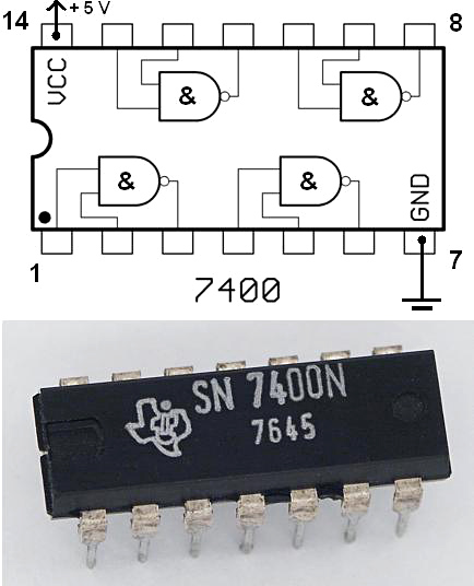
Our computer would end up pretty big if we started sticking dozens of those in even our simpler circuits. We might get it to a more manageable size using a bunch of 7400 series chips. Custom integrated circuits are the best way of cramming lots of transistors in a small space, but I don't have a semiconductor fab in my garage. For now I'll stick to HDL.
So given a bucket of NAND gates we're tasked with building the simplest logic gate: NOT.
# Not.hdl

CHIP Not {
   IN in;
   OUT out;

   PARTS:
   Nand(a=in, b=in, out=out);
}
That one is really simple. We just fork our in wire into both the a and b inputs on the NAND gate. A quick comparison of the NOT truth table makes it evident this will work:
NOT          NAND

in | out     a  | b  | out
--------     -------------
 0 |  1      0  | 0  |  1
             0  | 1  |  1
             1  | 0  |  1
 1 |  0      1  | 1  |  0
If in=0 then a=0 and b=0, so we get out=1.
If in=1 then a=1 and b=1, so we get out=0.
We've inverted the input.
I won't go into the solutions for all the chips here, but you can view my chapter 1 solutions on GitHub
It's like a puzzle though, don't look up the answers before trying yourself. It's really satisfying to finally figure some of these out. Hopefully the K-map trick will help you.